In physics, sputtering is a phenomenon in which microscopic particles of a solid material are ejected from its surface, after the material is itself bombarded by energetic particles of a plasma or gas.
Physical vapor deposition (PVD) is a vaporization coating technique, to deposit materials such as metals, ceramics, and plastics onto a surface (substrate) and to form a thin film. In general, it can be divided into two groups: sputtering and evaporation.
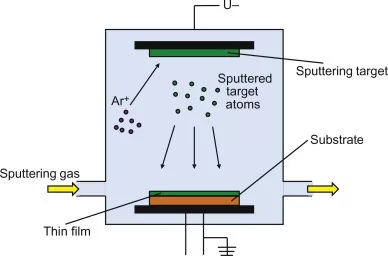
Sputtering is a physical vapor deposition (PVD) process used for depositing materials onto a substrate, by ejecting atoms from sputtering targets and condensing the ejected atoms onto a substrate in a high vacuum environment.
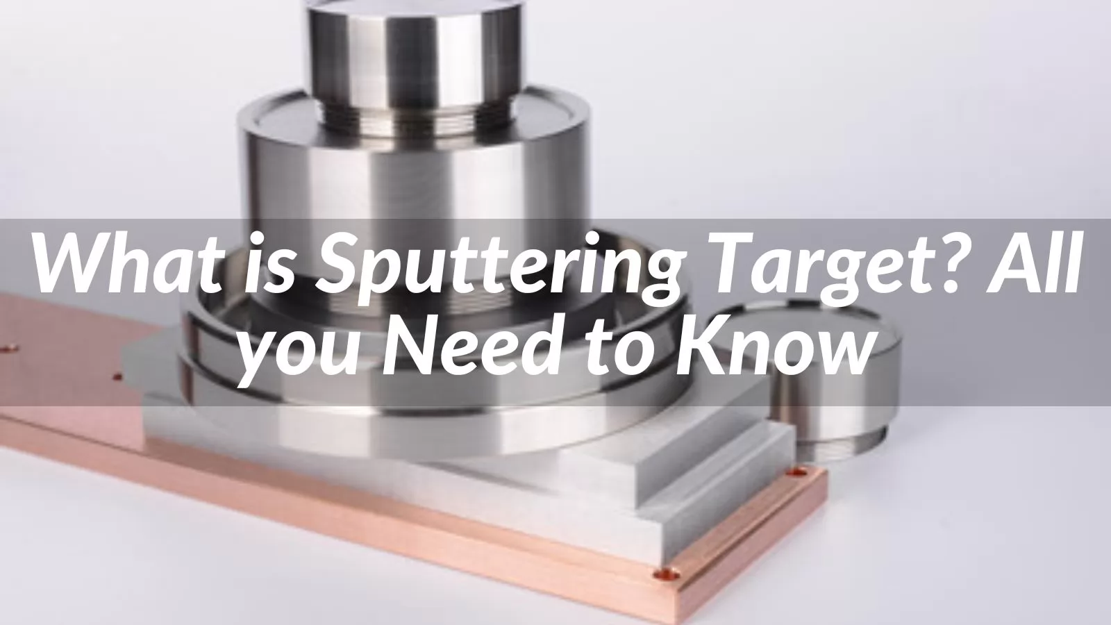
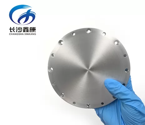
What is Sputtering Target?
A sputtering target is a crucial component used in the sputtering process, a widely employed technique in various industries such as electronics, semiconductor manufacturing, optical coatings, and thin-film deposition. In simple terms, sputtering is a process that involves the deposition of thin films onto a substrate by bombarding a solid target material with energetic particles.
The sputtering target acts as the source of the material that will be deposited onto the substrate. It is typically made of a high-purity material, often a metal or a compound, that matches the desired composition of the thin film to be formed. The target is placed in a vacuum chamber along with the substrate, and the sputtering process is initiated.
During sputtering, high-energy particles, such as ions or electrons, are accelerated and directed towards the target surface. When these particles strike the target, they dislodge atoms or molecules from its surface through a physical process known as sputtering. These sputtered particles then travel through the vacuum chamber and deposit onto the substrate, forming a thin film.
Sputtering targets are available in various shapes, sizes, and compositions to cater to different deposition requirements. They can be cylindrical, rectangular, or even custom-shaped, depending on the specific application. The choice of target material is crucial as it determines the properties of the resulting thin film, such as conductivity, optical characteristics, or chemical composition.
Composition of Sputtering Targets
Sputtering targets are composed of a wide range of materials, including metals, alloys, ceramics, and compounds, depending on the desired properties of the thin film to be deposited. The choice of target composition is critical as it directly impacts the characteristics and functionality of the resulting thin film.
Metal targets are one of the most common types used in sputtering processes. They are fabricated from pure metals or metal alloys and offer excellent electrical and thermal conductivity. Metals like gold (Au), silver (Ag), copper (Cu), titanium (Ti), and aluminum (Al) are frequently used as sputtering target materials. These metal targets are ideal for applications such as semiconductor fabrication, display coatings, and solar cells.
Ceramic targets are composed of non-metallic materials, typically oxides, nitrides, or carbides. Examples of ceramic sputtering targets include aluminum oxide (Al2O3), titanium dioxide (TiO2), silicon dioxide (SiO2), and zinc oxide (ZnO). Ceramic targets are known for their high melting points, chemical stability, and dielectric properties, making them suitable for applications in optical coatings, wear-resistant films, and protective layers.
Compound targets are composed of two or more elements, resulting in a mixture or compound material. They offer unique properties and are used to deposit thin films with specific functionalities. Examples of compound sputtering targets include indium tin oxide (ITO), a transparent conducting oxide used in touch screens and displays, and chromium nitride (CrN), a hard and wear-resistant coating material.
The composition of sputtering targets can be tailored to achieve desired properties such as electrical conductivity, optical transparency, corrosion resistance, or magnetic characteristics. Manufacturers often provide a wide range of target compositions to meet the diverse requirements of different industries and applications.
It's important to note that the composition of the sputtering target directly affects the composition of the deposited thin film. Therefore, careful selection of the target material is crucial in achieving the desired thin film properties and performance.
Manufacturing Process of Sputtering Targets
The manufacturing process of sputtering targets involves several steps to ensure the production of high-quality, precise, and reliable targets. The process may vary depending on the type of target material and the specific requirements of the application. Here is an overview of the typical manufacturing process:
1. Material Selection:
The first step in manufacturing sputtering targets is the careful selection of the material. The material is chosen based on the desired properties of the thin film to be deposited. Factors such as conductivity, composition, purity, and compatibility with the deposition process are taken into consideration.
2. Material Preparation:
Once the material is selected, it undergoes preparation. In the case of metal targets, the material is usually in the form of a high-purity ingot. The ingot is then processed through various techniques such as melting, casting, or powder metallurgy to obtain the desired shape and size of the target. Ceramic targets are typically manufactured through powder processing methods like solid-state reaction, sol-gel, or plasma spray.
3. Shaping:
The prepared material is shaped into the desired target form. This can involve processes like machining, grinding, or pressing. Machining is commonly used for metal targets, where the material is cut or drilled to achieve the desired dimensions and surface finish. Ceramic targets may undergo grinding or pressing to obtain the desired shape and density.
4. Finishing:
After shaping, the target goes through a finishing process to ensure the required surface quality and dimensional accuracy. This can include polishing, lapping, or chemical treatments. The goal is to remove any surface imperfections or contaminants that may affect the target's performance during sputtering.
5. Quality Control:
Throughout the manufacturing process, rigorous quality control measures are implemented to ensure the targets meet the specified requirements. This includes material analysis, dimensional checks, purity verification, and overall target quality assessment. Targets that do not meet the set standards are rejected to maintain the highest quality standards.
6. Packaging and Delivery:
Once the sputtering targets pass the quality control checks, they are carefully packaged to protect them during transportation and storage. Special care is taken to prevent damage or contamination. The targets are then shipped to the customers, ready to be used in their sputtering processes.
The manufacturing process of sputtering targets requires precision, expertise, and adherence to strict quality standards to ensure the production of targets that deliver consistent and reliable performance in thin-film deposition applications.
What are the Sputtering Technologies?
1) Magnetron Sputtering
Magnetron sputtering is a widely used sputtering technique that enhances the efficiency and control of the sputtering process. In this method, a magnetic field is applied near the sputtering target to trap electrons and increase the plasma density. The magnetic field, typically created by permanent magnets or electromagnets, forms a closed loop around the target surface.
When a voltage is applied between the target and the substrate, the magnetic field confines the electrons near the target surface, leading to a higher ionization rate and more efficient sputtering. Magnetron sputtering offers advantages such as improved target utilization, higher deposition rates, better film uniformity, and the ability to sputter a wide range of materials. It is commonly used in industries such as electronics, optics, and coatings.
2) Reactive Sputtering
Reactive sputtering is a technique that involves sputtering a target material in the presence of a reactive gas, typically a gas containing oxygen or nitrogen. The reactive gas reacts with the sputtered atoms or molecules, leading to the formation of compound films. This process enables the deposition of materials that cannot be directly sputtered in their pure form.
Reactive sputtering is extensively used for depositing oxide, nitride, or carbide thin films. It offers precise control over film stoichiometry and allows the tailoring of film properties such as composition, hardness, and refractive index. Reactive sputtering finds applications in areas like optical coatings, corrosion protection, and semiconductor devices.
3) Ion Beam Sputtering (IBS)
Ion beam sputtering (IBS) is a specialized sputtering technique that utilizes a highly focused ion beam to sputter the target material. In this method, a high-energy ion beam bombards the target surface, causing sputtering and the ejection of target atoms. The ions used in IBS are typically generated from an ion source.
IBS offers advantages such as precise control over film thickness, high deposition rates, and the ability to sputter a wide range of materials. It is particularly suitable for the deposition of high-quality, dense, and smooth thin films, making it a preferred choice for applications in optics, precision optics, and coatings where excellent film quality is crucial.
4) Focused Ion Beam Sputtering (FIBS)
Focused ion beam sputtering (FIBS) is a specialized form of ion beam sputtering that combines sputtering and ion milling with focused ion beams. In FIBS, a finely focused ion beam is used to sputter and mill the target material with exceptional precision. The focused ion beam can be scanned across the target surface to create complex patterns or perform material removal with high spatial resolution.
FIBS is commonly used in applications such as microfabrication, circuit editing, and sample preparation for transmission electron microscopy (TEM). It enables precise material removal, deposition, and modification at the micro- and nanoscale, making it a valuable technique in various research and manufacturing fields.
5) Electron Beam Sputtering
Electron beam sputtering is a sputtering technique that employs a focused electron beam to sputter the target material. In this method, a beam of high-energy electrons bombards the target, resulting in the ejection of target atoms or molecules. The sputtered species then travel through the vacuum chamber and deposit onto the substrate.
Electron beam sputtering offers advantages such as high deposition rates, precise control over film thickness, and the ability to sputter a wide range of materials. It is commonly used for depositing complex multilayer structures, optical coatings, and thin films with exceptional adhesion and density.
Each of these sputtering technologies has its own unique characteristics and advantages, making them suitable for different applications and deposition requirements in industries such as electronics, optics, energy, and materials science.
Types of Sputtering Targets
Sputtering targets are available in various types, each designed to meet specific deposition requirements and applications. Here are some of the commonly used types of sputtering targets:
1. Metal Targets:
Metal targets are one of the most widely used types of sputtering targets. They are fabricated from pure metals or metal alloys and offer excellent electrical and thermal conductivity. Metal targets are commonly used for applications such as semiconductor manufacturing, thin-film deposition, optical coatings, and magnetic storage media production. Examples of metal targets include gold (Au), silver (Ag), copper (Cu), aluminum (Al), and titanium (Ti).
2. Ceramic Targets:
Ceramic targets are composed of non-metallic materials, typically oxides, nitrides, or carbides. Ceramic sputtering targets are known for their high melting points, chemical stability, and dielectric properties. They are widely used in applications such as wear-resistant coatings, optical films, and thin-film resistors. Examples of ceramic targets include aluminum oxide (Al2O3), titanium dioxide (TiO2), silicon dioxide (SiO2), and zinc oxide (ZnO).
3. Alloy Targets:
Alloy targets are sputtering targets composed of a mixture of two or more metallic elements. Alloy targets offer the advantage of tailoring the properties of the deposited thin films by adjusting the composition of the alloy. They are used in a range of applications, including magnetic recording media, superconducting films, and corrosion-resistant coatings. Examples of alloy targets include nickel-chromium (NiCr), titanium-aluminum (TiAl), and cobalt-chromium (CoCr).
4. Composite Targets:
Composite targets are sputtering targets made by combining different materials or layers to achieve specific film properties or multilayer structures. They are often used in applications where precise control over film composition and structure is required. Composite targets find applications in areas such as optical filters, solar cells, and integrated circuits.
5. Customized Targets:
Customized targets are tailored to meet specific customer requirements. These targets can be made from unique compositions, shapes, or sizes to address specialized applications. Custom sputtering targets are commonly used in research and development, prototyping, and niche industries where standard targets may not suffice.
It's worth noting that the type of sputtering target chosen depends on factors such as the desired film composition, the deposition technique, and the specific application requirements. Manufacturers often provide a wide range of target options to cater to diverse industry needs and enable precise thin-film deposition.
Applications of Sputtering Targets
Sputtering targets find extensive applications in various industries that rely on thin-film deposition. The versatility and precise control offered by sputtering technology make it a preferred choice for numerous applications. Here are some key areas where sputtering targets are commonly employed:
1. Semiconductor Manufacturing:
The semiconductor industry extensively utilizes sputtering targets for the deposition of thin films in the fabrication of integrated circuits (ICs) and other semiconductor devices. Sputtered films are used for applications such as barrier layers, interconnects, dielectric layers, and metal contacts. Metal targets like aluminum (Al), copper (Cu), and tungsten (W) are commonly employed in semiconductor manufacturing.
2. Optics and Optical Coatings:
Sputtering targets play a critical role in the production of optical coatings for various applications. They are used to deposit thin films on optical components, such as lenses, mirrors, filters, and waveguides, to enhance their performance in terms of reflectivity, transmittance, anti-reflection, and color control. Materials like indium tin oxide (ITO), titanium dioxide (TiO2), and silicon dioxide (SiO2) are widely used in optical coating applications.
3. Energy and Solar Cells:
The energy sector utilizes sputtering targets for applications such as solar cells, fuel cells, and energy storage devices. Sputtered films are used to create transparent conductive layers in solar cells, enabling efficient light absorption and charge transport. Materials like indium tin oxide (ITO) and aluminum-doped zinc oxide (AZO) are commonly employed as targets in solar cell manufacturing.
4. Display Technologies:
Sputtering targets are vital for the production of displays, including flat panel displays (LCD, OLED), touch screens, and flexible displays. They are used to deposit transparent conducting films, color filters, reflective layers, and electrode materials. Indium tin oxide (ITO), indium gallium zinc oxide (IGZO), and aluminum (Al) are commonly used targets in display technologies.
5. Wear-resistant and Decorative Coatings:
Sputtering targets are employed to create wear-resistant coatings on various surfaces, including cutting tools, molds, and automotive parts. These coatings enhance hardness, wear resistance, and corrosion resistance. Additionally, sputtering targets are used for decorative purposes, such as in the production of decorative films on jewelry, watches, and architectural glass.
6. Magnetic Storage Media:
Sputtering targets are crucial in the manufacturing of magnetic storage media, such as hard disk drives (HDDs) and magnetic tapes. They are used to deposit thin films of magnetic materials, such as cobalt (Co), nickel (Ni), and iron (Fe), which form the recording layer that stores data magnetically.
These are just a few examples of the wide-ranging applications of sputtering targets. The flexibility, precision, and control offered by sputtering technology make it a vital process in industries that require the deposition of high-quality thin films for various functional and protective purposes.
Conclusion
Sputtering targets play a fundamental role in the process of thin-film deposition through sputtering. They are essential components used in various industries such as semiconductor manufacturing, optics, energy, and electronics. Sputtering targets are meticulously manufactured with high precision and are available in different types, including metal targets, ceramic targets, alloy targets, composite targets, and customized targets.
If you want to know more, please contact us!


.png)


.png)

 info@xk-sputteringtarget.com
.png)
.png)

.png)
.png)
 Hot Article
.png)