What Are Sputtering Targets? Understanding the Backbone of Thin Film Deposition
_1691377040_WNo_465d400.jpg)
Sputtering targets are essential components in the world of thin film deposition, a crucial process used in various industries to create thin layers of materials on substrates. These targets serve as the source from which atoms or molecules are ejected during the sputtering process, facilitating the deposition of thin films onto desired substrates.
Types of Sputtering Targets: Unraveling the Diversity in Thin Film Deposition
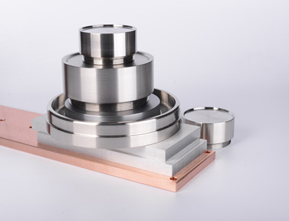
Sputtering targets play a critical role in the process of thin film deposition, offering a diverse range of materials suited for specific applications and industries. The types of sputtering targets available cater to the unique needs and demands of various sectors, making them indispensable components in modern manufacturing processes.
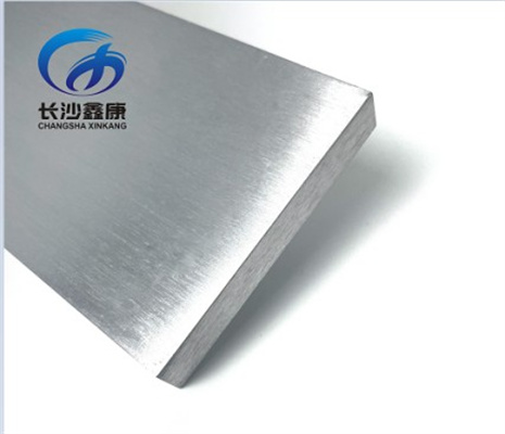
1. Metallic Sputtering Targets: Powering Electronics and Optics
Metallic sputtering targets consist of pure metals or metal alloys, each chosen for its specific electrical, thermal, or optical properties. These targets find extensive use in the electronics and optics industries, where precise and reliable thin film deposition is crucial.
2. Ceramic Sputtering Targets: Precision in Semiconductor Manufacturing
Ceramic sputtering targets consist of non-metallic compounds, primarily oxides, nitrides, and carbides. These targets are extensively used in semiconductor manufacturing, where precise and controlled thin film deposition is crucial for device performance.
3. Alloy Sputtering Targets: Tailored Properties for Specific Needs
Alloy sputtering targets are composed of two or more metals, combined to create unique and tailored properties. These targets find applications in specialized industries that require specific material characteristics.
4. Composite Sputtering Targets: Combining Advantages
Composite sputtering targets consist of a mixture of different materials, combining their individual advantages to meet specific application requirements.
What are sputtering targets used for? Multiple Applications of Thin Film Deposition
Sputtering targets are invaluable components in the field of thin film deposition and are used in numerous industries and technical applications.
1. Semiconductor Industry: Electronic Devices
2. Display technology: light up the screen
3. Optics and Coatings: Enhanced Vision and Function
4. Data storage: storing information
5. Photovoltaics: Harnessing solar energy
6. Wear and Corrosion Protection: Maintain Durability
7. Decorative paints: beautify everyday objects
8. Research and Development: Enabling Innovation
The Sputtering Process: Unveiling the Key to Precise Thin Film Deposition
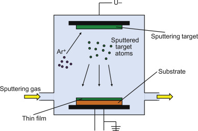
The sputtering process is a fundamental technique used in thin film deposition, allowing the controlled transfer of material from a sputtering target to a substrate. This versatile and widely adopted process plays a pivotal role in numerous industries, from semiconductor manufacturing to optics and beyond.
1. Understanding Sputtering: A Particle Bombardment Technique
At its core, sputtering involves bombarding a sputtering target with high-energy ions or neutral atoms. These energetic particles collide with the surface of the target, dislodging atoms or molecules from the target material. The ejected particles then travel through a vacuum chamber and deposit onto a substrate, forming a thin film layer with properties dictated by the target material.
2. Magnetron Sputtering: Enhancing Efficiency and Uniformity
One popular variant of the sputtering process is magnetron sputtering, which utilizes magnetic fields to enhance the efficiency and uniformity of thin film deposition. The presence of magnetic fields in the sputtering chamber traps electrons, leading to an increased ionization rate and improved target utilization. Magnetron sputtering is favored for its ability to produce high-quality and dense films with excellent adhesion to the substrate.
3. Reactive Sputtering: Expanding Material Choices
Reactive sputtering is another essential form of the sputtering process. In this technique, a reactive gas, such as nitrogen or oxygen, is introduced into the sputtering chamber alongside the inert gas. The reactive gas interacts with the ejected target material, allowing the creation of compound thin films with unique properties. This process expands the range of available materials and opens up new possibilities for tailored thin film characteristics.
4. DC Sputtering vs. RF Sputtering: Power Sources
The sputtering process can be further classified based on the power source used:
4.1. DC Sputtering: DC sputtering employs a direct current power source to create the electric field necessary for ionization. It is a simple and cost-effective method commonly used in research and smaller-scale production.
4.2. RF Sputtering: RF (radiofrequency) sputtering utilizes radiofrequency power to generate the electric field. RF sputtering is more efficient and offers greater control over the sputtering process, making it suitable for large-scale production and industrial applications.
5. Sputtering Parameters: Fine-Tuning the Process
The sputtering process is highly controllable, allowing researchers and manufacturers to fine-tune various parameters to achieve specific thin film characteristics. Key parameters include sputtering power, target-substrate distance, gas pressure, and deposition time. Each parameter can influence the film's thickness, density, adhesion, and microstructure.
6. Substrate Selection: Influencing Thin Film Properties
The choice of substrate material is crucial in thin film deposition. The substrate's surface properties and temperature significantly impact the nucleation and growth of the deposited film. Proper substrate selection ensures adhesion and compatibility with the intended application.
7. Applications of Sputtering Process: Driving Technological Innovations
The sputtering process finds diverse applications in various industries:
✓ Electronics: Used to fabricate conductive and insulating layers in semiconductor devices.
✓ Optics: Essential for producing advanced optical coatings and thin-film mirrors.
✓ Data Storage: Key in the manufacture of thin-film magnetic heads for hard disk drives.
✓ Solar Energy: Enables the production of thin-film solar cells for efficient photovoltaics.
✓ Displays: Used to create transparent conducting layers in flat-panel displays.
FAQs (Frequently Asked Questions)
Q1. What are sputtering targets made of?
A1. Sputtering targets can be made of various materials, including pure metals (e.g., gold, aluminum, titanium), ceramic compounds (e.g., silicon dioxide), alloys (e.g., copper-indium-gallium-selenium), and composites (e.g., carbon nanotube composites). The choice of material depends on the specific application and desired thin film properties.
Q2. How does sputtering work?
A2. Sputtering is a particle bombardment technique where high-energy ions or neutral atoms collide with a sputtering target, ejecting material from its surface. The ejected particles then deposit onto a substrate, forming a thin film.
Q3. What industries use sputtering targets?
A3. Sputtering targets find applications in various industries, including semiconductor manufacturing, electronics, optics, data storage, solar energy, aerospace, and decorative coatings.
Q4. What is the difference between DC and RF sputtering?
A4. In DC sputtering, a direct current power source is used to create the electric field necessary for ionization, while RF sputtering employs radiofrequency power. RF sputtering is more efficient and allows greater control over the sputtering process, making it suitable for large-scale industrial applications.
Q5. What is the importance of substrate selection in thin film deposition?
A5. Substrate selection is crucial as it influences the adhesion and compatibility of the deposited thin film. The substrate's surface properties and temperature significantly impact the nucleation and growth of the film, affecting its final characteristics.
Q6. What are some advantages of using sputtering targets for thin film deposition?
A6. Sputtering targets offer several advantages, including:
High purity, ensuring consistent and reliable thin films.
Excellent adhesion, resulting in robust and durable coatings.
Tailored properties, allowing the customization of thin film characteristics for specific applications.
Q7. How thin are the deposited films in sputtering?
A7. Sputtering enables the deposition of thin films with thicknesses ranging from a few nanometers to micrometers, depending on the application and requirements.
Q8. What are the applications of sputtering in the electronics industry?
A8. In the electronics industry, sputtering is used to fabricate conductive, insulating, and barrier layers in integrated circuits, microchips, and thin film transistors (TFTs). It also plays a crucial role in producing interconnects, electrodes, and contacts for electronic devices.
Q9. How does reactive sputtering differ from conventional sputtering?
A9. Reactive sputtering involves introducing a reactive gas (e.g., nitrogen or oxygen) during the sputtering process, leading to the creation of compound thin films with unique properties. Conventional sputtering uses only inert gases like argon.
Q10. What future trends can we expect in sputtering target technology?
A10. Future trends in sputtering target technology may include the development of novel target materials, improvements in target manufacturing techniques, and advancements in magnetron sputtering processes to achieve even higher efficiency and control.


.png)


.png)

 info@xk-sputteringtarget.com
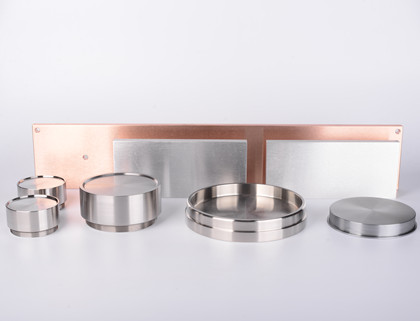


.png)

.png)